Design rule check (DRC)
Locate the following files and copy them into ~/ER_ASIC_Rev1/APR for ease of use:
- Standard:
~/65nm_PDK_ZIP/65 MS RF GP/DRC Command File/Mentor Graphics/.../ MAIN_DRC_TopMu/CLN65S_9M_6X1Z1U.26_2a
- Antenna:
~/65nm_PDK_ZIP/65 MS RF GP/DRC Command File/Mentor Graphics/.../ ANTENNA_DRC/CN65S_9M_ANT.26_2a
- MiM Antenna:
~/65nm_PDK_ZIP/65 MS RF GP/DRC Command File/Mentor Graphics/.../ ANTENNA_MIM_DRC/CN65S_9M_6X1Z1U_MIM_ANT.26_2a
- Wirebond:
~/65nm_PDK_ZIP/65 MS RF GP/Package DRM and DRC/Wirebond/DRC/ Mentor Graphics/.../GOLD_WIRE_BOND_DRC/65nm/ CN65_WIRE_BOND_9M_6X1Z1U.14a1
The MiM antenna file may not be required if there are no MiM capacitors in your design. The ERASICv1 did not have any MiM capacitors.
TSMC will require the latest DRC deck, which was 2.6.2a in April 2026. You may have to request the latest version from MUSE, and they will send you the files via Box.com. Additionally, in the standard DRC file, comment out #DEFINE WLCSP_SEALRING.
In the ASIC_Tapeout layout, navigate to Calibre → Run nmDRC. Select the previously used runset (e.g., Dummy_Runset) and save as a new runset with a different name (e.g., DRC_Runset). The following image shows the DRC dialog:
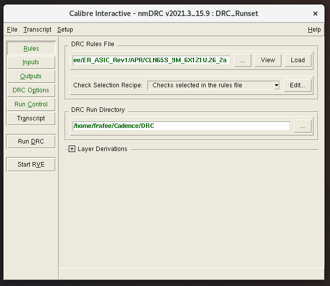
Make the following changes in the dialog to differentiate the files by <NAME>:
- Rules
- DRC Rules File:
~/ER_ASIC_Rev1/APR/CLN65S_9M_6X1Z1U.26_2a
- DRC Rules File:
- Outputs
- DRC Results File:
ASIC_Tapeout_<NAME>.drc.results - Format: ASCII
- DRC Summary File:
ASIC_Tapeout_<NAME>.drc.summary
- DRC Results File:
The critical deliverables from these DRC runs are the summary files. Be sure to save each summary file with a different name.
After these modifications, save the runset and select "Run DRC." Repeat this process for all four files, changing the DRC Rules File selection and <NAME> accordingly.
DRC errors
Waivable DRC errors
Once DRC completes, an RVE window will open with the results. Ideally, all DRC errors should be eliminated before tapeout. However, several DRC errors are likely to be waiveable by the foundry if they are not critical errors. A list of previously successfully waived errors follows:
- M(n).DN.(n), OD.DN.(n): This is the general form of density type errors. One example is `M8.DN.1'. These are errors generated when the filler scripts didn't quite meet the density requirements. As long as the density is close, the error should be waived. Typical errors occur on M8 and M9, and on OD (OD.DN.2L, OD.DN.3L, etc.).
- LUP.2g: These are "latch-up violations" which are usually generated in the ADC. Since the I/Os are ESD protected, this is not an issue.
- ESD.(n): These are general ESD violations. Violations are thrown for the I/O cells themselves, which are of course not modifiable.
All DRC waiver requests must be documented in the DRC Waiver Request Presentation provided by MUSE. More information on can be found later.
Unwaivable DRC errors
The DRC tool provides basic feedback on how or why the errors occurred, and it is up to you to decipher and understand how to resolve the error. In rare cases, you may be forced to make hand modifications to the design in Cadence to resolve the error, but this should only be used as an extreme last resort. Some known error cases are detailed below:
- I/O VSS/VDD vias: Innovus routes VSS and VDD from the I/O pads to the internal power and ground rings during top-level routing. Since the routing tool is unaware of the vias in the I/O pads, it automatically places vias to make connections to the pads. With two sets of vias overlapping, DRC will throw errors. To resolve this, manually delete the via blocks after importing the GDS into Cadence.
- Interconnect antenna violations: Antenna violations occur when there is a large area of one particular metal layer connecting to a single gate. During fabrication, the large metal area will incur a large current due to ion deposition which may destroy the transistor. Innovus handles these errors, so none should occur within the digital core. However, the large interconnects between the ADC and digital core (or any other modules, depending on the design) may cause antenna errors. To resolve this, break up the connections onto different metal layers. For example, if the connection is all on M5, just add a short bridge onto M6 and then back to M5 to break up the metal area.
- SRAM connections: Connections made to SRAM blocks, or wires routed around SRAM blocks will be unaware of the specific metal routing inside the block. As such, DRC errors may arise nearby to the SRAMs. Although fixes to this issue have not been tested, one solution that may help is to increase the "halo" region, or protected unroutable area, around the SRAM.
Density DRC errors
If the density is close but not exactly meeting, it can usually be waived. MUSE will need an image of the error in the layout, the required density value, and the achieved density value.
To find the achieved density value, in the RVE window, click on the error and right click on the name of the error, which is highlighted in blue. Click on "Highlight Result ID." The following image shows this button in the RVE window:
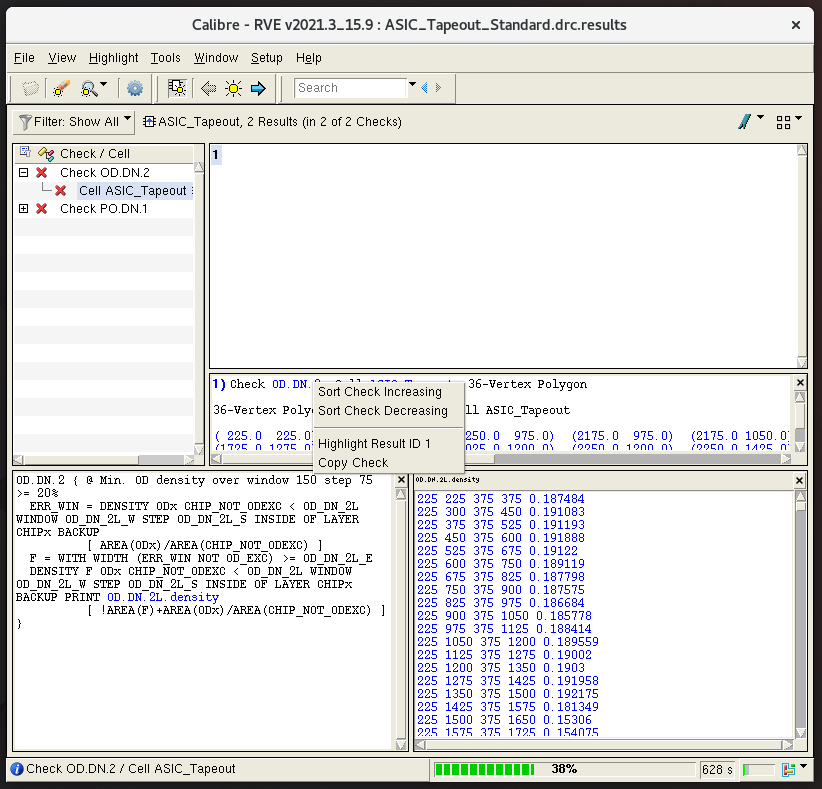
In the Layers panel on the left side, click on "NV" to turn off visibility of displayed layers. The area that doesn't meet the density requirement will be and flashing. Take a screenshot to include in the DRC Waiver Request Presentation.
To find the density in this area, navigate to Tools → Area and Density Calculator. In the dialog, change "Layer" to the layer of interest. For region, select the last option and click on the red button to select a polygon region. The following image shows the dialog with the selections:
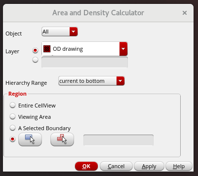
In the layout, carefully trace out the dashed line and hit the "Enter" button on your keyboard when you've finished. In the dialog, click "OK" and another dialog will appear, indicating the density.