Pad-level module
Create a module called DigitalCorePads that instantiates the "logical" top-level (DigitalCore), as well as the I/O pads. You will also need a dummy holder for PCORNER that can be included in the RTL folder of DigitalCorePads. Look at previous code for reference.
You will need to indicate how many pads you want for DVDD (VDDPST), DVSS (VSSPST), VDD, and VSS. Note that one of the VDDPST pads will need to be VDDPST (POC), which is the pad VDD2POC instead of VDD2DGZ. POC stands for "power-on control" and is needed to monitor the power-on sequence. Ensure that this is accounted for in DigitalCorePads.
Additionally, there should only be one input port for each I/O VDDPST and VSSPST so that one unified power net connects to all VDDPST/VDDPST pins across all pad instances. The core VDD and VSS can just be global nets.
The total number of pads in your design may not be the same as the total number of pins. For example, in the ERASICv1, there are 32 pins, but 49 pads because there are 7 VSS pads and 10 VSSPST pads. Ground pins are not required because the ground pads can connect to the substrate. The following image shows the pin diagram on the left and the pad diagram on the right for the ERASICv1:
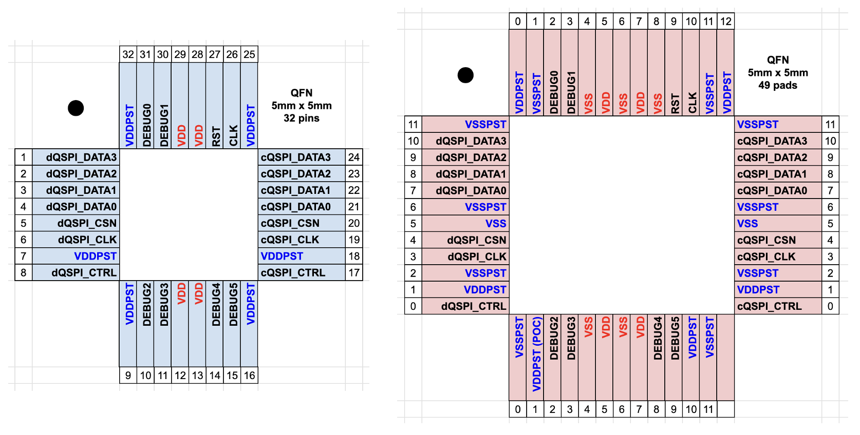
The north edge has 13 pads while the east, south, and west edges have 12 pads. This allows TSMC to easily distinguish the orientation of the chip.