Chip-level assembly
Create bond-pad level layout
In the Library Manager, select the library you created and navigate to File → New → Cell View. Name the cell ASIC_ALL, and select the view to be "layout." The Virtuoso Layout Suite will open.
Navigate to Create → Instance (or click i on your keyboard) to create an instance of a cell. For cell, select DigitalCorePads, and for view, select "layout." Line up the bottom left corner with the origin.
Create bond pads
Now, we want to add the bond pads. The bond pad option we will use is circuit under pad (CUP) I/O, which is the I/O with the bond pad over the I/O body itself. The pad pin is located closer to the center of the chip and should be connected to the I/O pin. The following image shows PAD60GU, one of the bond pads included in the standard cell library:

The pad pin, which is at the top of the previous photo, will need to oriented closer to the center of the chip and will be aligned with the I/O pins in the linear bond style. Create another instance of a cell, but select PAD60GU and check the box for "Create as mosaic." For "rows/columns," type the number of pads on that edge, and for "delta y/x," type the spacing for that edge using the number that was printed to the terminal earlier when generating the TCL script for APR. Rotate and align it accordingly.
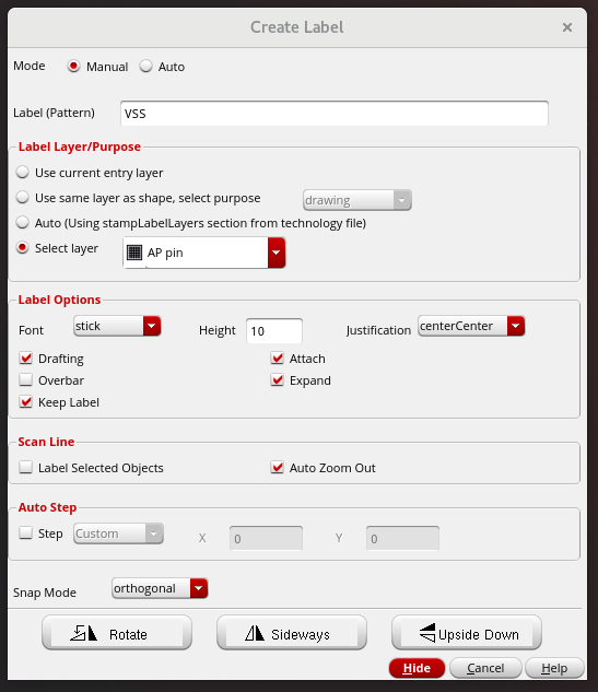
Create bond pad labels
Now, we want to add the labels. Navigate to Create → Label (or click l on your keyboard) to create a label. Name it accordingly, select the AP pin layer, and increase the font height. The naming convention should match that of the TCL script generated for APR. Place it over the bond-pad. A dialog will appear, prompting you to "choose object for label creation." Select "PAD60GU (mosaic)." Repeat for all pads.
The following image shows the bond pad label for one bond pad:
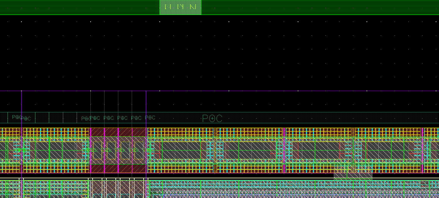
Create POC pin
You will also need to create a pin for the POC pad in the ASIC_ALL layout to pass LVS. Navigate to the PVDD2POC pad and zoom in on the rings towards the inside of the I/O pads. You will find the POC rail on the M3 layer labeled with POC. Create a label, and name it "POC", select the M3 pin layer, and decrease the font height if needed. Place it over the POC metal. The following image shows the placement of the POC pin label:
Final result (ASIC_ALL)
The following image shows the final result of ASIC_ALL for the ERASICv1, which includes DigitalCorePads, the bond pads, and the bond pad labels:
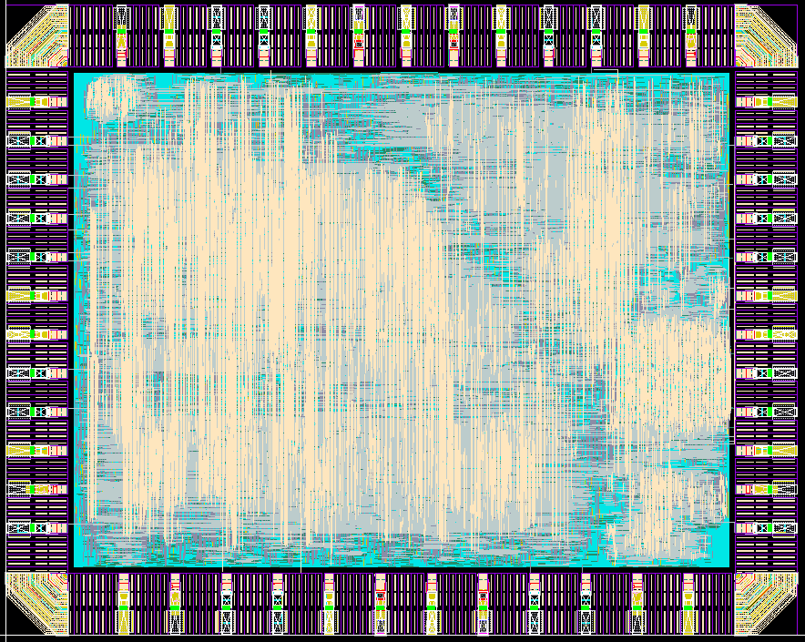
Layers M7, M8, and M9 are hidden for aesthetic purposes.